Transistor schematic
Logic
Level
3
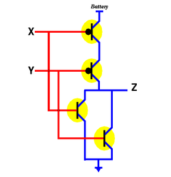 Which of the following functions is represented by the above transistor schematic?
Z = X NAND Y
Z = X NOR Y
Z = X OR Y
Z = X AND Y
This section requires Javascript.
You are seeing this because something didn't load right. We suggest you, (a) try
refreshing the page, (b) enabling javascript if it is disabled on your browser and,
finally, (c)
loading the
non-javascript version of this page
. We're sorry about the hassle.
Whenever X or Y is 5 V( or both), one of the transistors becomes ON and hence Z is grounded(0 V). But if both of them are 0 V, both transistors are OFF and hence Z is directly connected to the source battery and hence Z=5 V. This is indirectly the digital logic NOR gate. (Basic Digital Electronics)